

3KW high efficiency on board DCDC
Release time:
2023-05-16 18:19
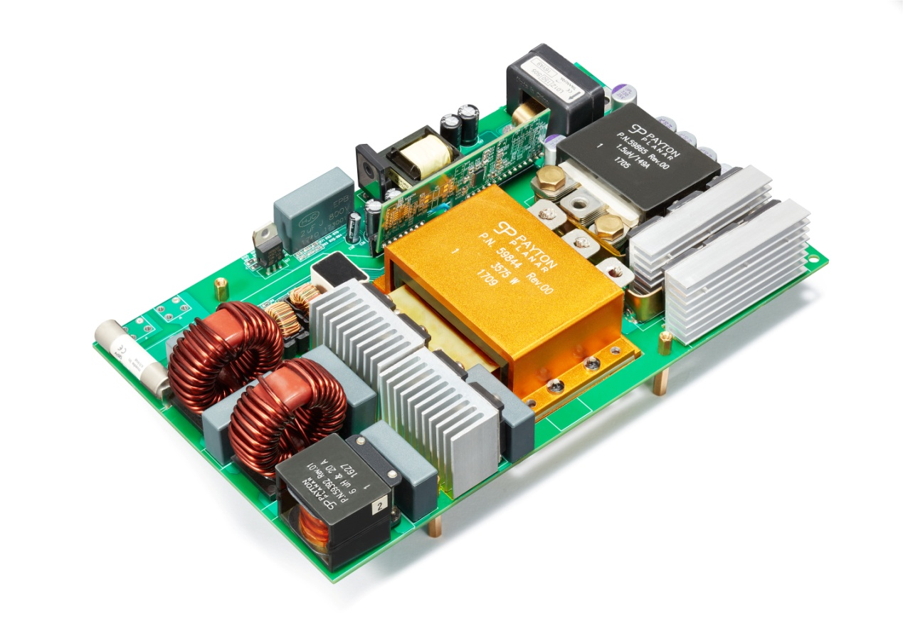
| Input Voltage | 350vdc-700Vdc |
| Output Voltage | 27.5Vdc |
| Rated Power | 3000OW |
| System Efficiency | Peak 96%: 93%@full load |
| Switching Frequency | 100KHZ |
FEATURES
· PSFB + Sync Rectifier base on SiC, simple & reliable system;
· High efficiency, peak up to 96%;
· Suitable for wide range output applications;
· Small volume (145mm235mm*45mm): power density 30W/incha3;
· Full protection, including input OVP, UVP & OCP, BUS OVP, output OVP.UVP & OCP, Short circuit protection, etc:
MAIN TOPOLOGY
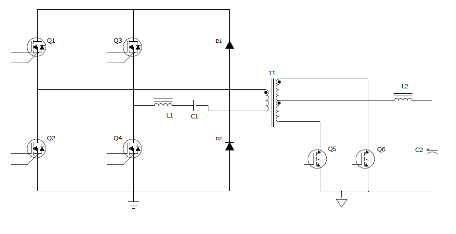
| Function | Part Number | Brand |
| Primary SIC MOSFET | C3M0120100K | Wolfs peed |
| Claim Diode | C4D05720A | Wolfs peed |
| Secondary MOSFET | IXFH90N20X3 | Wolfs peed |
| Primary MOSFET Driver | IXDN604SIA | Littelfuse |
| SecondaryMOSFET Driver | IXDN609SIA | Littelfuse |
MEASUREMENT RESULTS AND WAVEFORMS
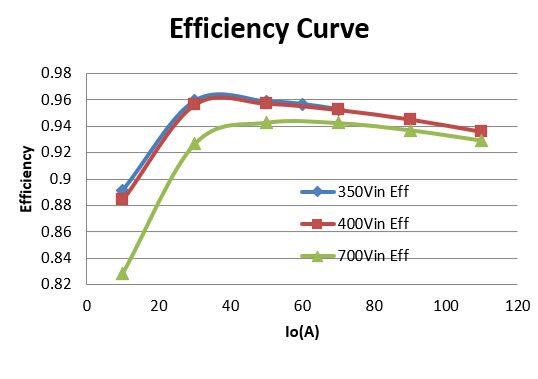
Efficiency Curve
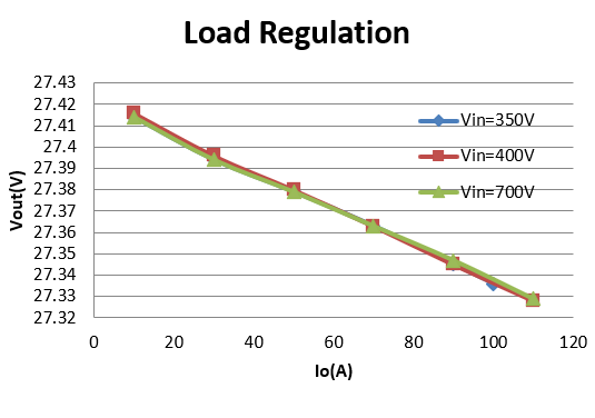
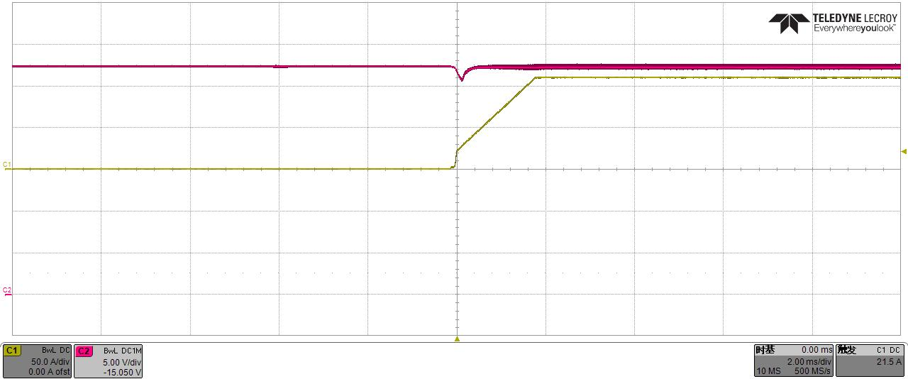
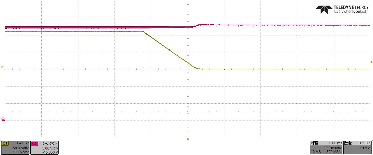
Load regulation
 350Vin 超前臂 ZVS
 700Vin 超前臂ZVS
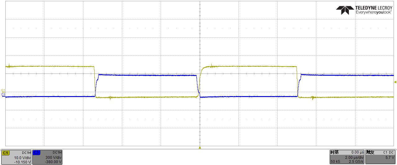
 350Vin lead leg Zvs
 700Vin lead leg ZVS
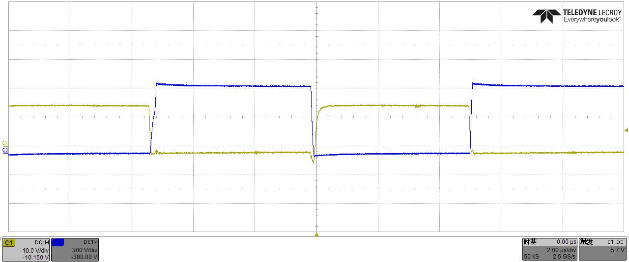
 350Vin lag led Zvs
 700Vin lag leg ZvS
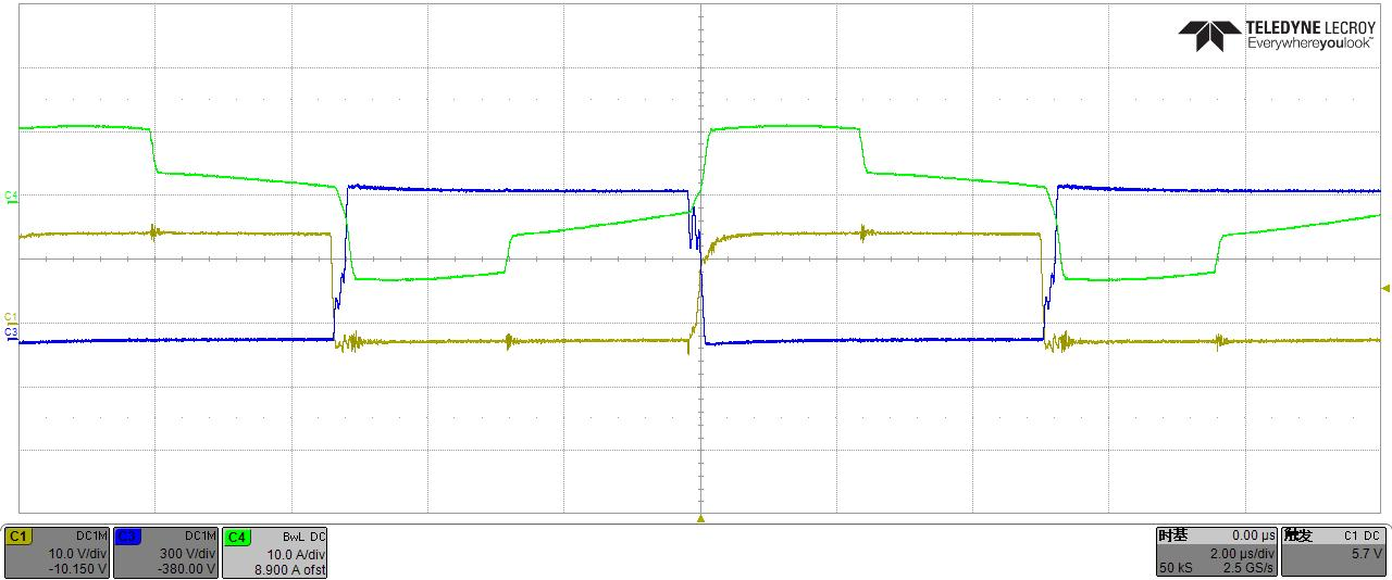
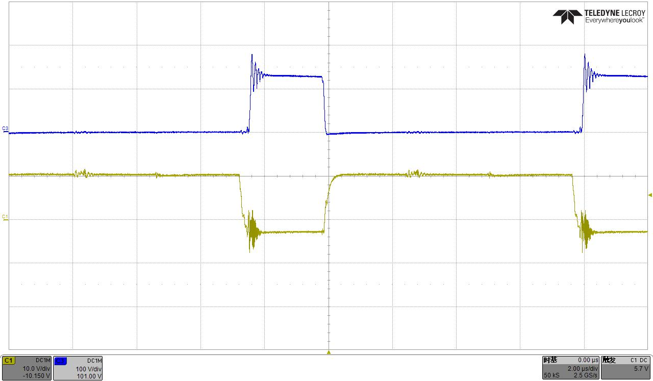
 350Vin Sync. MOSFET's Vgs&Vds
 700Vin Sync. MOSFET's Vgs&Vds
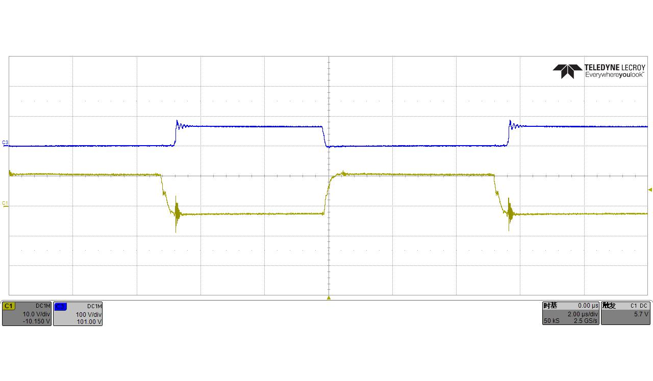
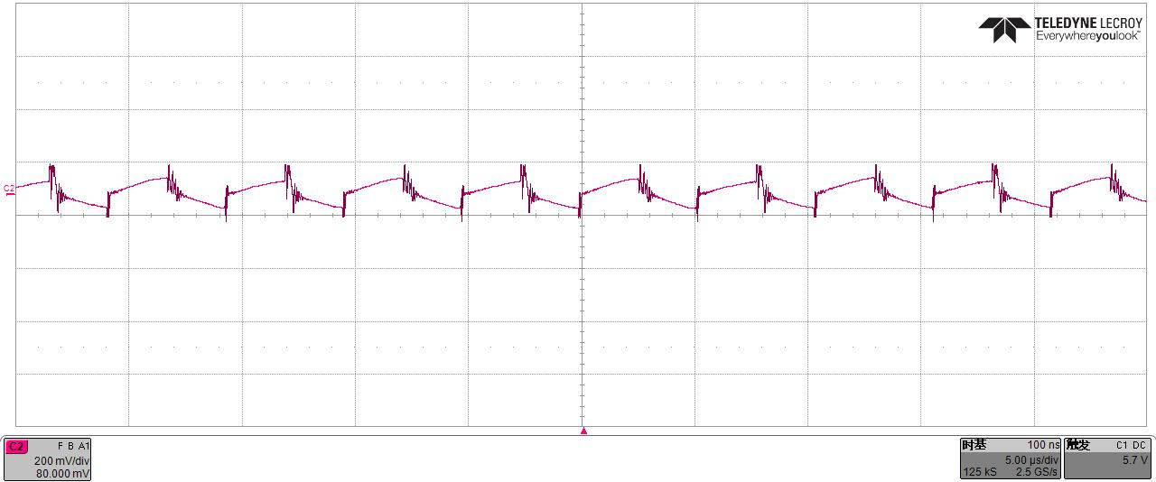
 Output voltage ripple @700Vin no load
 Output voltage ripple @700Vin full load
Download related files
3KW high efficiency on board DCDC
2023-05-24


official account